Intel redefines the chip industry with advanced packaging in New Mexico
Intel's New Mexico site is revolutionizing chipmaking with advanced packaging, scaling AI solutions beyond the industry's physical limits.
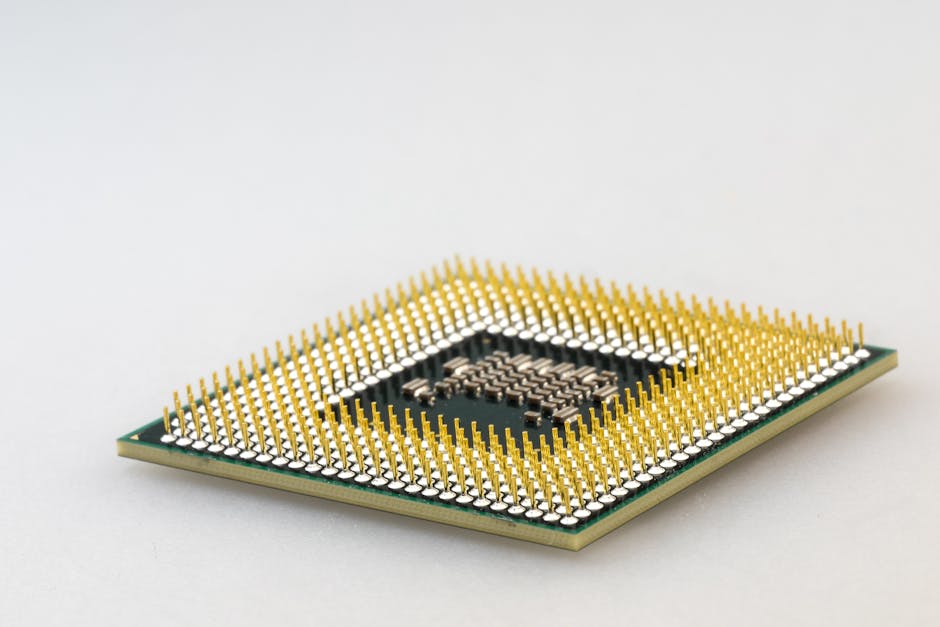
Silicon chips form the backbone of modern technology, powering everything from smartphones to data centers. Yet the increasing demands of artificial intelligence (AI) and other resource-intensive applications are pushing traditional chipmaking techniques to their limits. Intel is responding to this challenge with transformative advancements in chip packaging at its facility in Rio Rancho, New Mexico. This site, once a landmark in 6-inch wafer production, is now an industry leader in advanced packaging, a critical innovation that could define the future of computing.
Advanced packaging: breaking the single-chip mold
For decades, chip design followed a straightforward trajectory: build a single, larger chip to meet higher performance needs. That era is now being redefined by advanced packaging. Instead of relying on one monolithic chip, advanced packaging combines multiple specialized tiles into a cohesive "silicon mosaic,” enabling the creation of systems that are more powerful, flexible, and efficient.
This shift is particularly vital as AI demands have grown exponentially. Traditional manufacturing methods, constrained by the physical limits of lithography and wafer design, increasingly fall short. Intel has responded with breakthroughs like Foveros stacking, a 3D packaging solution that layers chips vertically, and EMIB (Embedded Multi-die Interconnect Bridge), which facilitates high-speed communication between chips.
Scaling beyond limits
Perhaps the most striking achievement at Intel’s New Mexico site is its ability to surpass the industry’s so-called reticle limits. Reticle limits refer to the maximum size of a single chip that can be produced in a typical photolithography system. Intel's packaging technology enables chip packages that are eight times the size of today’s industry standard. By 2028, Intel projects scaling this to over 12 times.
This is a game-changing development, significantly expanding performance potential without requiring costly and impractical investments in new lithography systems. These oversized chip packages are tailor-made for AI workloads, where the need for integrating massive data flows and processing power is paramount.
The New Mexico legacy
Intel’s Rio Rancho site has come a long way since its opening in 1980, when it consisted of 25 employees focused on wafer manufacturing. Now, with a workforce of 2,700 and a network of 500 suppliers, the facility plays a pivotal role in Intel's advanced packaging efforts. The team in New Mexico has turned the site into a global hub for cutting-edge innovation, squarely placing the U.S. on the map as a leader in critical semiconductor technology.
This comes at a time of heightened focus on semiconductor manufacturing in the United States. Intel’s investment in Rio Rancho aligns with the broader industry push to reduce reliance on overseas fabrication and build domestic capability. By spearheading advanced packaging here, Intel is not only positioning itself as a technology leader but also contributing to national economic and strategic goals.
Meeting the demands of AI
AI applications require chips that can handle vast amounts of parallel computations and transfer data quickly between processing units. Traditional designs, where individual chips perform isolated functions, are less suited to these requirements. Intel’s advanced packaging creates interoperable systems within a single package, reducing latency and power consumption—essential for AI workloads.
For instance, a high-performance AI chip might consist of multiple elements: one optimized for dense matrix calculations, another for memory access speed, and another for energy-efficient processing. With innovations like Foveros and EMIB, Intel integrates these components seamlessly, maximizing efficiency and performance.
Building customer trust
Intel isn’t just innovating for itself; the company sees this work as a cornerstone in its strategy to regain trust from major customers, particularly those in the AI and high-performance computing sectors. By delivering groundbreaking packaging solutions first to its clients, Intel aims to solidify its position as the go-to foundry for advanced silicon needs.
Trust is earned, and Intel's history of both leading and faltering in the industry underscores how critical this moment is. When the company delivers on its promises, particularly in AI-driven markets, it will reaffirm its role as a trusted supplier in a competitive semiconductor landscape.
The road ahead
With global demand for advanced semiconductors showing no sign of slowing, Intel’s focus on advanced packaging seems like the right bet. By designing solutions that sidestep the traditional limitations of chip manufacturing, Intel is not only meeting current AI demands but also paving the way for future breakthroughs. The Rio Rancho facility, once a small hub of innovation, has become the heart of an effort that could reshape computing as we know it.
As the industry moves closer to 2028, the scaling forecasted from this site—surpassing 12 times today’s reticle limits—aims to push AI capabilities further than many thought possible. Whether it’s self-driving cars, advanced robotics, or next-generation data centers, the era of advanced packaging will enable the technologies that define the next frontier.
Staff Writer
Maya writes about AI research, natural language processing, and the business of machine learning.
Comments
Loading comments…


